Hardware Hacking - Dumping Flash Memory of a TrendNet-731BRv1 Router
About The Project
Continuing on Arch Cloud Labs’ hardware and router reverse engineering journey, I wanted to dump the firmware of my TrendNet-731BRv1 via reading flash memory from the PCB vs downloading the firmware from TrendNet’s website. Considering a scenario where the firmware was no longer hosted publicly by TrendNet, (after all it is a discontinued product) being able to dump firmware off of a device is not only useful for situations dealing with deprecated hardware but also for poking at weird devices you might find at a garage sale or DEF CON’s IoT/Embedded Village.
This blog post will cover using an EEPROM Programmer to read the contents of a flash memory chip on the TrendNet-731BRv1 Router.
Recon On The Device - FCC ID & Hardware Identification
To dump the firmware from an embedded device, you must first find where it is stored. Multiple forms of storage can be on an embedded device, but the low-end routers I’m reverse engineering don’t have anything particularly crazy going on besides the possibility for USB storage or a microSD card to serve as some sort of NAS functionality. Going into this device, I’m looking for some kind of EEPROM/flash memory chip to dump data from.
Before cracking open a device to identify components, it’s possible to leverage existing photographs by the FCC to then look up the pin-out diagram of the chip. Any wireless device for sale in the United States requires said device to be registered with the Federal Communications Commission. This registration process results in a unique id per device, often referred to as a device’s “FCC ID”. Searching for a given device’s FCC ID will often result in photos of hardware teardowns of said device. FCCID.io provides an easy interface to search for said FCC ID which is obtained from somewhere on the hardware itself or a user manual.
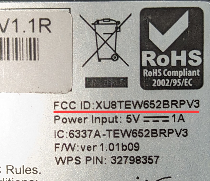
A quick search of the FCC ID highlighted in red above returns the FCC report for said device. As a part of the FCC certification, internal photos are taken of the device and are available in the FCC reports. Depending on the quality of the photos, this can help identify some surface-level components before you tear apart a device. I’ve annotated the image below with the red numbers of the various chips that are on the device. However, the quality of the FCC photos is not good enough to make out any identifying numbers to look up the data sheets of these chips. The data sheets will have pinout diagrams to understand how to hook up the IC test clip to the chip to then read data from the flash.
I did want to point out the UART silk screening on the board. In the FCC photos, there are headers already soldered on to the board, but on the hardware I have there are no UART headers. Probably due to a debug unit being used for FCC validation.
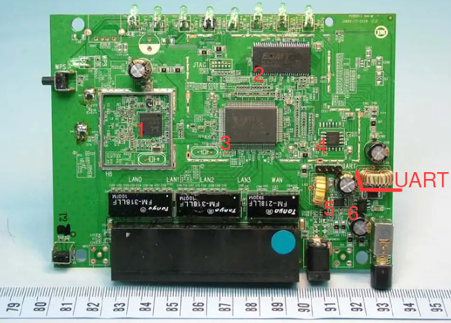
In the photo above, the following ICs ended up being:
-
ESMT M12L2561616A-6T - RAM for the device.
-
RealTek RTL8196C - System-on-a-Chip (SoC) this is the board’s processor.
-
MX25L3206E Flash Memory <– ding ding ding
-
Could not read the markings on the chip.
-
Could not read the markings on the chip.
Chip Pinout & Connecting the Programmer
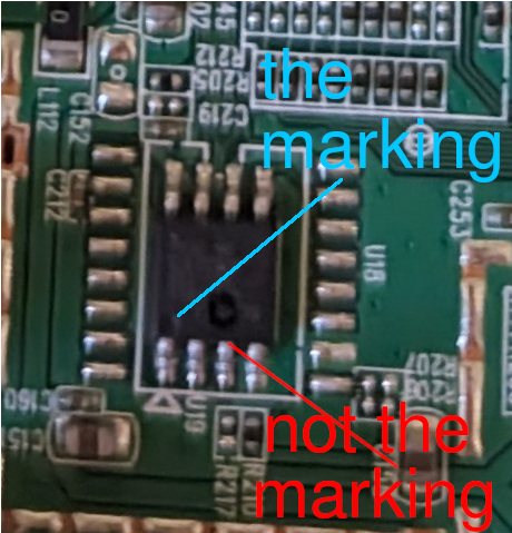
After identifying the MX25L3206E flash chip, the pin-out diagram in the data sheet shows the layout for both the 8-pin and 16-pin versions of this flash chip. The TrendNet-731BRv1 has the 8-pin version, so we don’t need to worry about having a 16-pin adapter. The image below shows the 8-pin layout with a black dot marking indicator where “pin 1” begins.
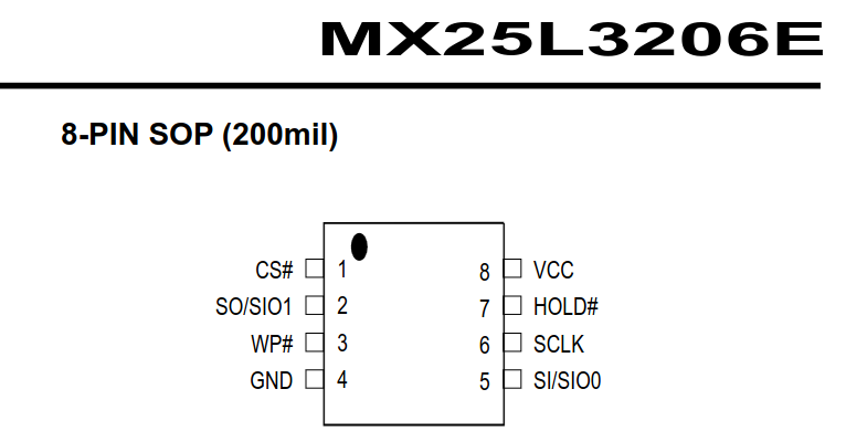
The IC test clip has one red cable to identify which pin is the “first pin”, this needs to correspond with the “dot” highlighted in blue on the chip pin-out diagram. Identifying this marking ensures appropriate connections to then use a flash programmer to interact with the integrated circuit.
With the pinout understood, now we can move onto hooking up the programmer and IC test clip to the board to begin reading memory.
Dumping Flash Memory
The Linux utility Flashrom is a utility for reading/writing flash chips. Per the official website, it supports more than 476 flash chips and 17 USB devices including the EEPROM programmer I bought, the CH341A programmer. Upon connecting the IC test clip to the flash chip on the PCB and plugging into programmer into my desktop, the power LED on the board lit up. Excellent sign! It’s important to note you do not need to apply power to the board as the programmer will do that.
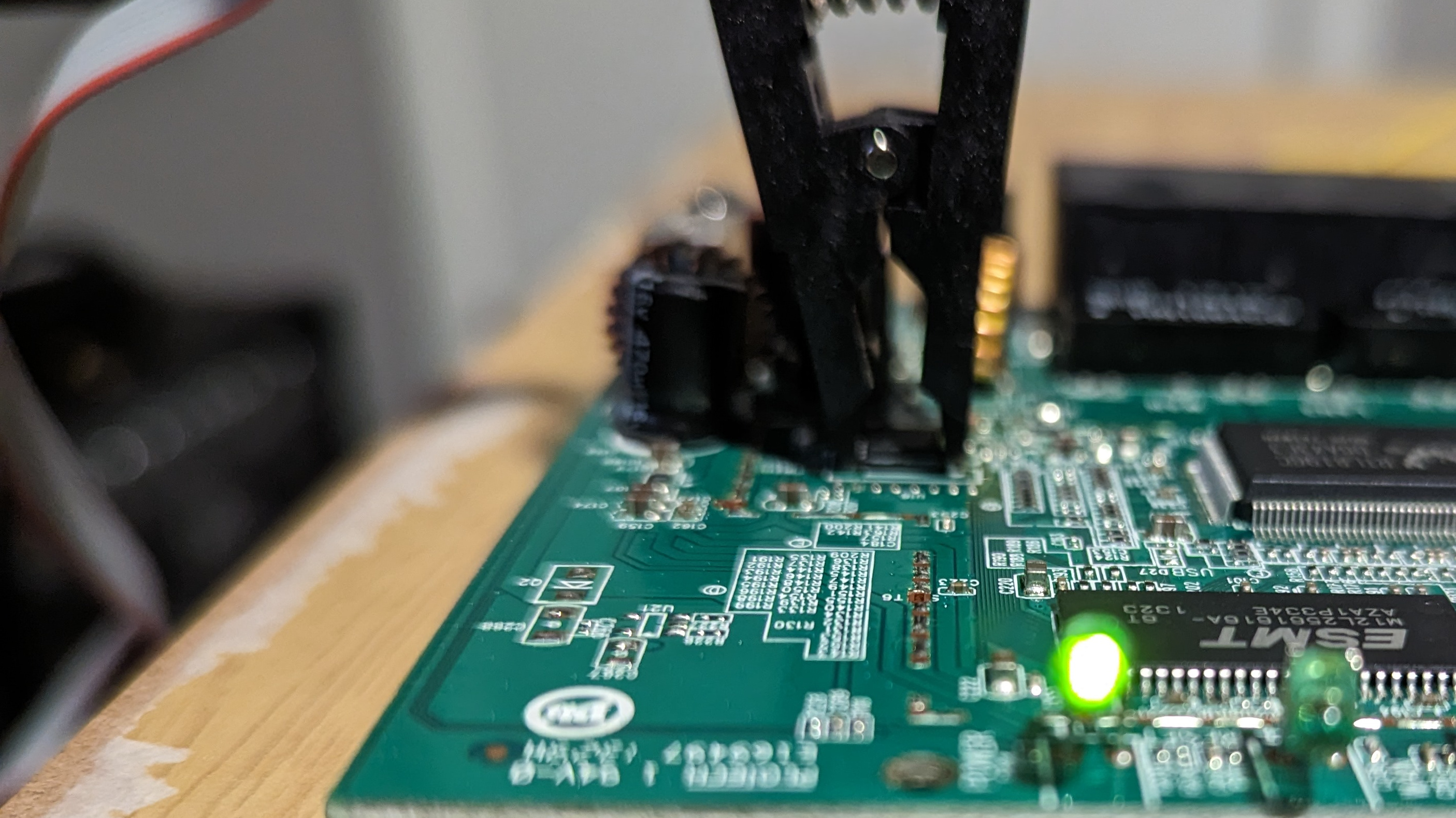
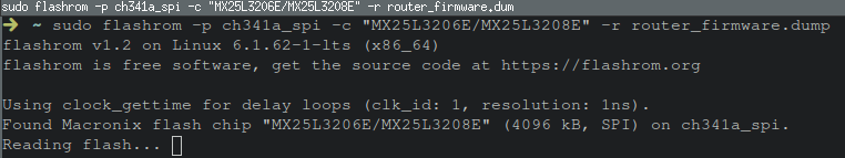
With the EEPROM connected and the IC test clip on the flash chip, Flashrom can recognize the connected flash chip (assuming it is supported) via just executing flashrom -p $PROGRAMMER_HERE. The example below shows that Flashrom identified potentially multiple chips, and this is where our previous device identification comes in handy to specifically specify the MX25L3206E/MX25L3208E option.
$> sudo flashrom -p ch341a_spi

flashrom v1.2 on Linux 6.1.62-1-lts (x86_64)
flashrom is free software, get the source code at https://flashrom.org

Using clock_gettime for delay loops (clk_id: 1, resolution: 1ns).
Found Macronix flash chip "MX25L3205(A)" (4096 kB, SPI) on ch341a_spi.
Found Macronix flash chip "MX25L3205D/MX25L3208D" (4096 kB, SPI) on ch341a_spi.
Found Macronix flash chip "MX25L3206E/MX25L3208E" (4096 kB, SPI) on ch341a_spi.
Found Macronix flash chip "MX25L3273E" (4096 kB, SPI) on ch341a_spi.
Multiple flash chip definitions match the detected chip(s): "MX25L3205(A)", "MX25L3205D/MX25L3208D", "MX25L3206E/MX25L3208E", "MX25L3273E"
Please specify which chip definition to use with the -c <chipname> option.
Flashrom can be used to read, write, and erase supported flash chips. In this case, I’m reading the flash memory and writing it to a local file to back up the firmware (aka dumping the firmware). This is achieved with the following flashrom syntax:
$> flashrom -p ch341a_spi -c CHIP_MAKE_AND_MODEL_GOES_HERE -r FILE_TO_DUMP_DATA_TO.
Executing the flashrom command on my local machine can be shown in the image below resulting in reading the memory from the flash chip.
Success!
The firmware has been dumped!
The command above dumped the data to router_firmware.dump which can then be carved up via dd or binwalk to extract embedded file systems. A quick execution of binwalk router_firmware.bin and cd’ing into the squashfs root directory, the same files explored in a previous blog post can be found.
➜ squashfs-root tree
.
├── bin
│   ├── acltd
│   ├── adduser -> busybox
│   ├── ash -> busybox
│   ├── auth
│   ├── auth-fail
│   ├── awk -> busybox
│   ├── brctl
│   ├── bunzip2 -> busybox
│   ├── busybox
│   ├── bzcat -> busybox
│   ├── cat -> busybox
│   ├── chmod -> busybox
│   ├── cp -> busybox
│   ├── crond -> busybox
│   ├── cut -> busybox
.....truncated......
Conclusion
This was my first time attempting to dump the firmware from a flash chip, but applying the techniques covered by Black Hills InfoSec and Dane Epp’s blogs on dumping firmware made me feel comfortable with breaking out a programmer and giving a go of my own. Hardware hacking always seemed like an expensive part of InfoSec to get in, but for less than twenty dollars USD (minus the cost of the target device), you too can begin dumping router firmware. Investing in a USB Microscope wouldn’t be a bad idea either considering how small some of the components are. I look forward to using this skillset at DEF CON next year and tackling some of the challenges at the IoT and Embedded Village. If you found this blog useful, please consider sharing it.